


 Although silicon-based semiconductors have transformed the world, creating the electronic age, they do have some shortcomings. For example, hard silicon components don’t bend or conform to tight or strange shapes, making them impossible for use in windshield-mounted displays or wearable electronics, and they are difficult to access for more complex jobs, like adjusting circuit frequencies, once they are made.
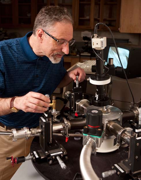
The solution, according to Howard Katz, chair and professor of materials science and engineering at the Whiting School, may be soft organic plastic electronics. Organic semiconductors are easy to manufacture, often cheaper than silicon, and can both absorb and emit visible light. Katz’s lab is developing transistors, diodes, sensors, and energy-converting devices such as solar cells, made from small molecule substances or long-chain polymers.
Organic semiconductors are based on research begun in the 1970s that went on to earn its inventors a Nobel Prize in chemistry in 2000. It is not possible to go inside silicon and carve out the chemistry needed for tasks more complex than simple switching, Katz says, while organic semiconductors can be constructed molecule by molecule, conforming to a task or form. Some organic and polymeric semiconductors can be bent or stretched over large areas, printed onto surfaces using ink-jet technology, or even spray-coated—deposited in ultra-thin films just a few molecules thick. They could also be used as electronic paper for a device like the Kindle, the electronic book reader, or to form arrays of microphones or solar cells.
Katz says organic semiconductors would be most effective in making sensors that can be deployed in places that rigid structures cannot reach. This would have broad ramifications for national security, for instance, for developing devices that can spot substances such as nerve gases and explosives. His lab is working on sensitive transistors that, exposed to targeted substances, would show changed electric currents flowing through them even if the substances are at concentrations less than one part per million. The interaction between the transistor and the targeted substance happens right where the current is, he says, something that is very difficult to do with a silicon device.
While it is relatively easy to produce plastic semiconductors that transport positively charged holes, it is much more challenging to produce devices that transport electrons, which is one of the specialties of Katz’s lab. Some circuits require both types, including solar cells, LED, and certain circuits, Katz says, which is why his lab is concentrating on the latter. The ability to work with both hole- and electron-carrying semiconductors opens up the possibility to make printed circuits more energy efficient, and also to expand the scope of energy conversion and storage devices, such as solar cells, thermoelectrics, and capacitors.