

Create
Design Project Gallery
CMOS Imager
- Program: Electrical and Computer Engineering
- Course: EN.520.216 Introduction to VLSI
- Year: 2025
Project Description:
This work presents the design, simulation, and layout of a CMOS active pixel sensor (APS) employing a three-transistor (3T) architecture with integrated column-parallel readout. Each pixel consists of a reset switch, source-follower amplifier, and row-select device, interfacing with a photodiode that generates a photocurrent proportional to incident illumination. A current-mode column readout circuit enables robust signal acquisition and biasing. Pixel functionality is validated through transient simulations utilizing modeled photocurrents and bias voltages. Row and column scanning are achieved using custom C²MOS shift registers to facilitate sequential raster readout. A 4×4 pixel array is implemented and laid out within a 2.5 mm × 2.5 mm die area, achieving full DRC and LVS compliance. The design demonstrates high fill factor, low-power operation, and scalability, providing a foundation for future monolithic CMOS imaging systems.
Project Photo:
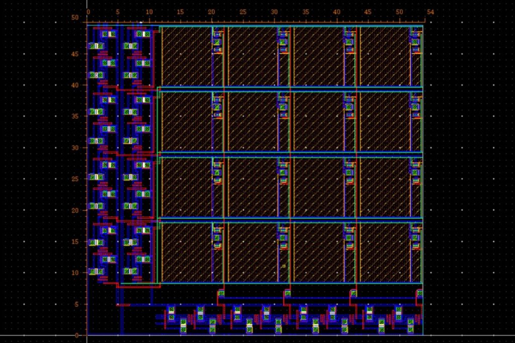
Final layout of a 4×4 CMOS active pixel sensor (APS) array with integrated C²MOS shift registers for row, column, and reset control. The design enables sequential raster readout through coordinated scanning logic, supporting low-power and scalable image sensing applications.