

Create
Design Project Gallery
CMOS Imager
- Program: Electrical and Computer Engineering
- Course: EN.520.216 Introduction to VLSI
- Year: 2025
Project Description:
This project presents the design, simulation, and layout of a CMOS active pixel sensor (APS) imager using Cadence tools. The imager includes a 3-transistor (3T) APS circuit, a 4×4 pixel array, and CMOS-based shift registers for row and column scanning. A single pixel and column read-out circuit were first validated individually. The design was expanded to demonstrate a full 4×4 array with photocurrents ranging from 1pA to 10pA to simulate varied light exposure. Raster scan readout was implemented using synchronized row and column shift registers. Emphasis was placed on maintaining layout constraints within a 2.5mm × 2.5mm area while passing DRC and LVS checks. Each pixel layout followed a 10µm × 10µm pitch, and fill factor was calculated accordingly. The final system integrates functional scanning logic and output multiplexing to deliver clear pixel signal readouts, demonstrating a compact, scalable architecture for future CMOS imaging applications.
Project Photo:
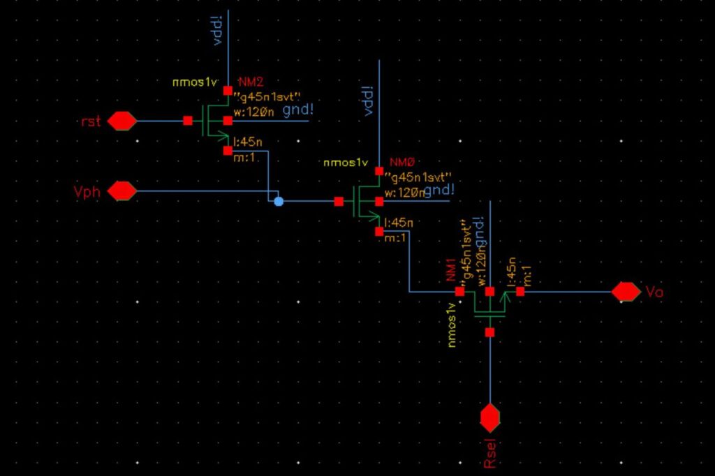
3T APS Pixel schematic