

Create
Design Project Gallery
3TAPS Camera Chip
- Program: Electrical and Computer Engineering
- Course: EN.520.216 Introduction to VLSI
- Year: 2025
Project Description:
This project involves the design, simulation, and layout of a CMOS image sensor using Cadence tools. Students will build and validate a 3-transistor active pixel sensor (3T APS), column and row C2MOS shift registers, and a column read-out circuit. The final design integrates a 4×4 pixel array with scanning logic and fits within a 2.5mm × 2.5mm layout. The imager will be tested through transient simulations showing pixel readouts. Deliverables include DRC/LVS-verified schematics, layouts, presentations, and a four-page IEEE-style final report.
Project Photo:
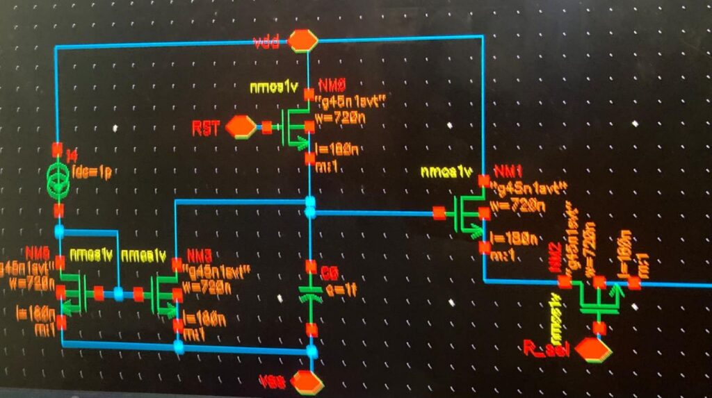
3TAPS Transistor