To create a new cell, click Library Manager:New -> Cellview. The create new file form should appear:
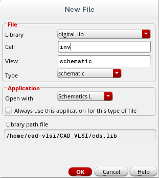
Note: The “Library path file” will vary based on your configuration.
We will be making an Inverter, so type inv in the Cell Name block. In the View Name block type schematic or from the Tool menu choose Composer-Schematic and the View Name Block will be automatically filled. Left click the OK button.
The Virtuoso-Schematic Editing window should appear on your screen.
We need to add components to the schematic. To do so, left click: Schematic Editing:Add ->
Instance (i).
Note: You may notice letters by some of these menu choices. Rather than clicking through all the menus, you can just hit that button on the keyboard to the same effect. These are called hot-keys or shortcuts. When applicable, we’ll list hot-keys after the menu choice instruction (as above, for Schematic Editing:Add -> Instance).
We’ll use a component given to us in the NSCU Analog Parts library: type NSCU_Analog_Parts in the Library Name box.
Type nmos4 to choose a four terminal NMOS transistor in the Cell Name box and symbol in the View Name box. This will allow us to place the symbol of an NMOS into our schematic. Note that you can use the Browse button in order to browse through the libraries and find the cell you want.
Move the cursor into the editing window. Notice that there is an NMOS transistor there instead of the normal cursor. Position it where you want to put the transistor, and left click to place it. You can right click to rotate the transistor if you want it to face a different direction (this is especially useful with pins).
Press Esc to return to a normal cursor after you have finished
placing all the transistors you want. For this inverter example, place it on the bottom half of the screen
on the right side of the center-line. To rotate press r.
Next, we’ll add a PMOS. Click Editing:Add ->Instance (i).
Follow the same steps as before, but choose a pmos4 transistor. Use the same values for length and width as the nmos4. Place the pmos4 transistor directly above the nmos4 transistor.
If the Add Component window is getting in your way, you can hid it: before trying to place a component, left click the Hide button on the Add Component window. This will move it into the background so it’s out of your way.
Now, we’ll add the pins for the inverter. Click Editing:Add->Pin (p).
The Add Pin dialog box comes up. In the Pin Names box enter all the pins: vdd, vss, in and out. Ensure that
Direction is set to inputOutput for all four pins (defining the pins like this makes things more
flexible, and won’t throw errors if a pin we’ve labeled output is driven, for example - this
means you have one less check on your work, so be careful!). The Add Pin window should look as follows:

Note that the order of the pin names is not important. You can also name one pin at the time, place the pin on the schematic and repeat the same procedure several times for placing the other pins. The end result will be the same.
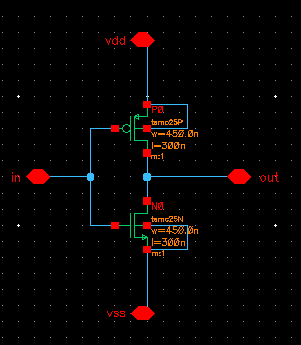
Following typical electronics conventions, place the vdd pin somewhere near the top of the editing screen, above the PMOS transistor. Then place the vss pin somewhere below the NMOS transistor. Place the in pin somewhere towards the left of the editing window, between the transistors. Place the out pin somewhere towards the right side of the editing window, between the two transistors
Now, we’ll add all the wires to make this inverter work. Click Editing: Add -> Wire
(w). The Add Wire form should appear. Just click its
Hide button. You can refer to the figure on the next page to see how everything is
connected together.
Notice that as you get closer to one pin than another (including those on devices), a small diamond will show up inside of or around that pin. That is where you want to click to connect a wire. Also, when wiring schematic, leave the wire width at 0, Route method at full, and (usually) Draw Mode as route. This tells that software to auto-route the wires for you.
For the first wire, left click on the gate terminal of the pmos4 transistor , and left click again on the gate terminal of the nmos4 transistor. You have just connected the gates.
Now, move the mouse until the little square is inside the diamond on the in pin. Left click in the diamond. Move the cursor over to the wire you connected the two gates together with. A diamond will form around the cursor, as long as it’s on the wire. Left click. You have just connected the input to the gates of both transistors.
Move the cursor up near the vdd pin. Left click inside the pin. Move the cursor to the source (the end with the arrow) of the pmos4 transistor (the end with the arrow). This will add the power line to the circuit.
Repeat the last paragraph with the vss pin, and the source of the nmos4 transistor. This gives current a return path to the power supply. The body of the nmos4 and pmos4 transistors are the center pins. On the pmos4 transistor, connect this pin to vdd. On the nmos4 transistor, connect the body to vss.
If you put a wire where you don’t want it to go, you can delete the wire by left clicking
Editing:Edit->Delete (d) and then left click on
the object you want to delete (wire, pin, component, etc. )
There should now only be one pin left on each transistor (the sources of both transistors). Connect these two pins together. Finally, connect this last wire to the out pin. A picture of what this should all look like is shown below.
Make sure your transistors size (w) and (l) match with the ones shown in this picture.
Once you are done editing, left click the “check mark” icon on the left side of the screen. This will
check your work for connection errors and will save your work in the library. You can accomplish the same
thing by left clicking Editing:Design -> Check and Save (s).