The symbol editor lets you create a “black box” description of a cell using labels, pins, shapes, notes, and a selection box. Symbols make your design more readable, as you can use them in more complex designs, instead of individual transistors.
In the Library Manager click once on the digital_lib library. Then left click Library Manager:File->New Cell. In the Cell Name type inv and in the View Name box type symbol. You can also click on the Tool box and select Composer-Symbol and the View Name box will be automatically filled.
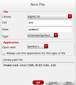
Left click OK
The Virtuoso Symbol Editing window should appear. You are ready to draw a symbol for the inverter. First, we will draw a triangle to represent the inverter body. Left click Editing: Add -> Shape -> Polygon
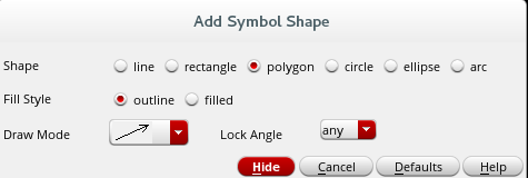
The Add Symbol Shape window appears. Left click Hide for now. To draw a polygon, click at a start point, and then click at the corners of the shape you want to create. To finish the polygon, click again on the start point. Since we are drawing an inverter, we need a sideways triangle, so make one of those. Look at the final picture at the bottom for guidance to draw.
The inverter needs a negation circle at the sideways corner of the triangle, so left click Editing:Add->Shape->Circle. Hide the Add Symbol window again. Left click at the point you want to be the center of the circle. Move the mouse until the circle is the size you want, and left click again.
Now draw a line that starts at the middle of the vertical line of the triangle and ends somewhere to it’s left and another line from the rightmost part of the circle to somewhere equally to the right, so left click Editing:Add->Shape->Line.
Hint: Rather than invoking the Add Symbol Shape box every time and having to go through the menus, leave the Add Symbol box in the foreground. When you are done drawing a shape, just left click on the appropriate radio button for the new shape you want to draw. When you are done, left click on Cancel to get rid of the box.
Now, you want to add pins to the symbol. Left click Editing:Add -> Pin
In the Pin Names box type the following pin names: vdd, vss, in and out. Also change the direction of the pins to InputOutput, and change the type to Square from actHi. After these changes the Add Pin window should look like this (except that the Type should be Square):

Click on the Hide button and you will return to the editing window. You are going to start placing the pins in the symbol in the order specified in the Pin Names box, i.e. first you will place the vdd pin, then vss and so on. The pins look a little different than the ones in the schematic, so be careful. You will notice that it is a box with a line attached. The end of the line will have the pin name. The box is the actual pin, so it must point AWAY from the rest of the symbol.
Now place all the pins around the symbol. Put the vdd pin on the top of the symbol and the vss pin on the bottom of the symbol. Add the out pin on the right and the in pin on the left of the symbol. The pins in ALL cell views of a single cell must have the same attributes and names. In other words, the input to the inverter in the schematic was called in and was an input/output pin. Therefore, the input pin on the symbol must also be named in and must also be an input/output pin. When you save your symbol, any differences between the pins of the symbol and the pins of the schematic will be reported as warnings. Following these warnings you can figure out where the inconsistency in the design has occurred.
Once you place the pins, the pin names may be hard to read for a variety of reasons. You can therefore move the pin name by clicking on the pin text label and then left click on Editing:Edit->Move. Now you can move the label and place where ever you want to. Next we want to add label to the symbol. Left click Editing: Add -> Label… The Add Symbol Label dialog box should appear.
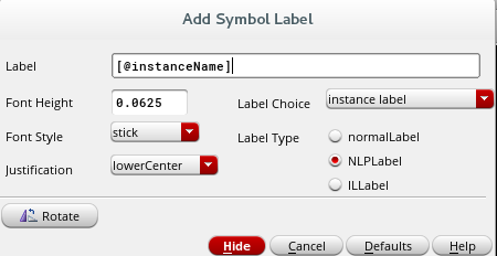
We will add two labels to the symbol. The first one is an instance label. Just left click the Hide button, and place the label somewhere near the symbol of the inverter.
Now, we need to add the normal label to the symbol. Left click Editing: Add -> Label…
Left click on the Label Type and select normalLabel and now type in the name of the device in the Label field. Hide the Add Label window, and place the label inside of the symbol. The first label was an instance label. Later, when you use symbols to build schematic, the software needs to know which symbol is which. It does this by looking at the symbol label, to see which kind of symbol it is. It them looks at the instance label to see which one of those it is. If you put multiple symbols into a schematic window, they will be labeled U1, U2, etc.
The last thing to add is a selection box. This will tell the software how much of the symbol is actually used.
Left click Editing: Add -> Selection Box…
Left click the Automatic button.
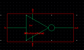
The symbol is now finish and you can save it by left clicking Editing:Design->Save. The symbol should look like the one below.