Now that we have built an inverter, we need to simulate it to show that our design is valid. Before proceeding with simulating the inverter circuit, we should create a new library for testing our digital circuits. This way we can separate out the primary digital cells from the test schematics. Create a new library called digital_lib_test in your working directory. Follow the same steps as describe earlier when creating the digital_lib library.
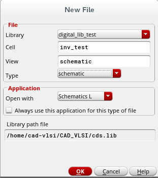
First we need to create a new cell in digital_lib_test library for testing our inverter. It is a good practice to keep separate your cell with your test files. In the Library Manager, highlight the digital_lib_test library and left click on Library Manager:File->New->Cell View.
In the Cell Name type inv_test and in the View Name type schematic. Left click on OK.
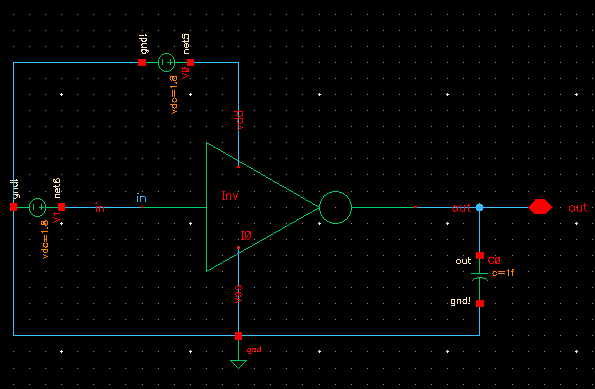
A new schematic editing tool will appear. You are going to instance the inverter that was previously created and connect its input and vdd pin to voltage sources. The output pin will be connected to a capacitor while the gnd pin will be grounded.
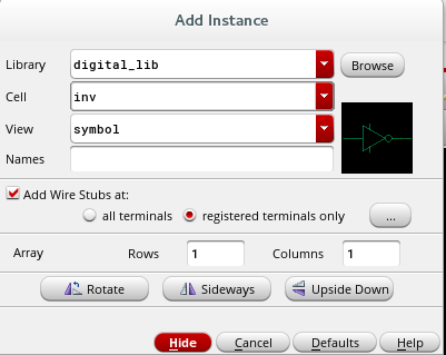
Left click Editing:Add->Instance. Click on the Browse button and using the Library Manager select from the digital_lib library, the inv cell, with symbol view. Then close the Library Manager. The Add Component window should look like this:
Place the inverter in the middle of the editing window. Now we want to add voltage DC sources. Left Click Editing: Add->Instance. In the Library Name field type NSCU_Analog_Parts; in the Cell Name type gnd and then place the symbol bellow the inverter. Left Click Editing:Add->Instance. In the Library Name field type NSCU_Analog_Parts; in the Cell Name type vdc; in the Cell View type symbol. In the DC Voltage field enter 1.8V. This window should appear as such:
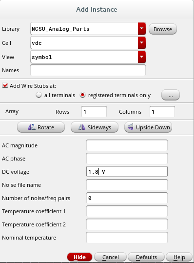
Place one copy of the voltage source above the inverter and one next to the input of the inverter. The value of the voltage source which will be connected to the input of the inverter is not important because this voltage source will be swept during the DC analysis.
We want to add capacitor to the output pin in order to simulate a load (other circuits) that our inverter has to charge or discharge. Left click Editing:Add->Component. From the NSCU_Analog_Parts library choose a cell named cap and specify its value to be 1fF.
Next we will add an output pin in the schematic. Left click Editing:Add->Pin?. Name the pin out and specify it as an input/output pin. Place the pin next to the output of the inverter.
Connect all the elements as shown in the figure bellow. To connect different elements use Editing:Add->Wire
Save the schematic and you are ready to simulate the inverter.