The tool for layout creation is called VIRTUOSO. In the Library Manager highlight the inv cell in the digital_lib library. Left click Library Manager:File->New->Cell View in the cell view of the inv type layout and click OK.
Two windows should have appeared. The Virtuoso Layout Editing window, and the LSW window. The LSW window is the one you will use to choose the different layers of the IC design. The LSW window is divided in three main categories which are: color, layer and purpose.
- Color: Matches the color in the Editing window. Each layer has its own color and pattern.
- Layer: What is the type of layer (Active, Metal1, Poly, Metal2, etc)
- Purpose: drw = drawing, pn = pin.
Each layer has two colors associated with it; a fill color and an outline color. These colors can be changed to fit your taste by editing the technology file.
Now we are going to build the layout of the inverter. An inverter has an NMOS and a PMOS transistor. First we will build an NMOS transistor.
You can use Ctrl-Z to zoom in and use Shift-Z to zoom out
Left click LSW: Active drw
Left click Editing: Create -> Rectangle
Left click: Hide
Notice that when the mouse is inside of the Editing window that the X and Y coordinate values (found between the title bar and the menu bar) change. These are very handy in making layouts. Also, notice the dX and dY items. When creating shapes, these show how far in each direction you have moved the cursor (since the last click).
From this point on, when I want you to click at a certain point in the Editing window, I will give you the X and Y coordinates in standard Cartesian form: (X,Y). If you make a mistake at any time you can left click on Editing:Edit->Undo. Also you can use move, copy, stretch and delete. Take some time to play with these controls and see how they work.
If you are unable to select the exact coordinates make sure your display is set to the right snap spacing. Left click Editing: Options -> Display and make sure X Snap Spacing is 0.09 and Y Snap Spacing is 0.09. This snaps the cursor to move in increments of 0.09 microns.
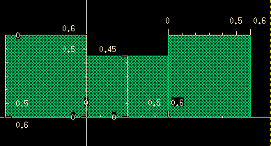
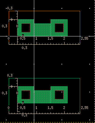
Draw a few rectangles to make the following shape of the PMOS diffusion.
The dimension of the rectangles of shown below. To get the ruler, Press
the hotkey K. To get rid of all the rulers, use the hotkey
Shift-K
Now we replicate the same diffusion for NMOS. You can press the left mouse key to select everything and press C to copy them.
[
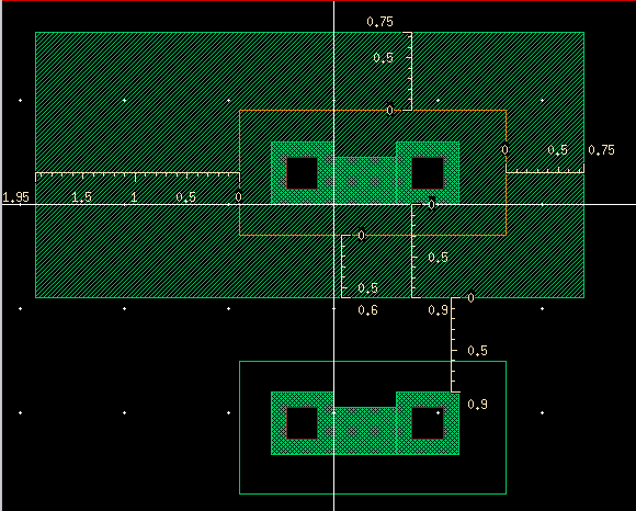
Now, let put the Metal_1 to diffusion contacts (also known as vias).
Left click LSW. cc drw
Left click Editing: Create -> Rectangle
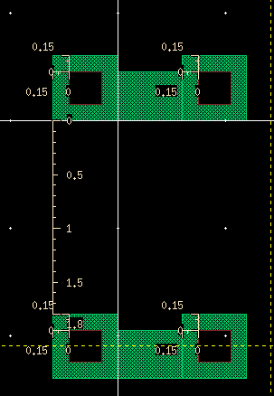
The dimension of the contacts are shown below:
Handy tip: When drawing many of the same things (rectangles, polygons, etc) you can just right click the mouse to repeat the last operation (draw rectangle, draw polygon, etc.)
A via connects the active region to a metal1 layer. A via cannot go through more than one layer. There are three different types of vias to connect all the from poly to metals, and between all 6 layers of metals in this process.
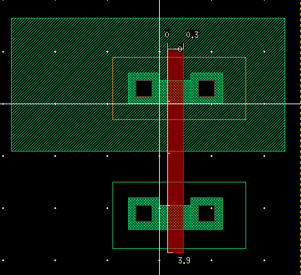
Now let’s draw the Pselect around the PMOS:
Left click LSW. Pselect drw
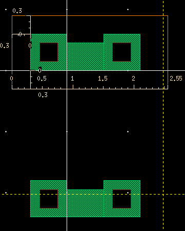
Everything (that’s visible) inside the Pselect (active) region will be doped as a P-type semiconductor (excess of holes). Since the transistor is of the N-type, it creates a diode junction between the N-doped regions and the P-substrate (The silicon wafer is P-type). This gives a direct connection into the substrate so that we can ensure that the diodes are reverse biased (no current will flow).
Now let's draw the Nselect for the NMOS
Left click LSW: Nselect drw
Now let’s draw the Nwell around the PMOS.
Left click LSW. Nwell drw
Now let’s draw the gates of the NMOS and PMOS using Polysilicon
Left click LSW: Poly drw
Now we have finished making the transistors. But all the transistors need Bulk connections. Now we will draw the bulk for NMOS and PMOS using the Diffusion, N-select, P-select, and Visa.
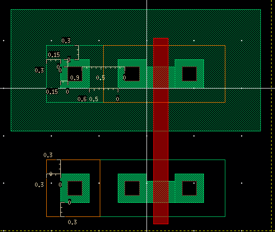
You have just finished building a NMOS and a PMOS transistor. Poly crossing active is a transistor. Where the poly actually crosses is the gate of the transistor. Everything we are doing is in units of microns Notice that the gate is 0.18 microns long. The smallest possible length of the gate is being used.
Now let’s connect all the terminal using Metal 1.
Left click LSW. Metal1 drw
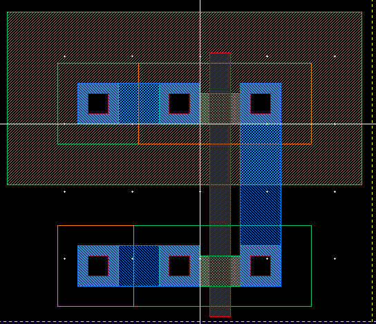
We have finished making an Inverter!
Now it is time to add pins. Pins are used to extract the layout and use it from LVS (layout vs. schematic) to ensure the layout match the schematic.
Left click LSW: Metal1 drw
Left click Editing: Create -> Pin… The Create Pin form should appear.
Ensure that I/O Type is set to inputOutput. It is important that this type matches the pin type used in the schematic to prevent warnings. Also make sure that Create label option is checked or otherwise the label names will not appear in the design. Ensure, also, that the Display Pin Name box is checked. Type vdd in the Terminal Names box. Make sure the mode is set to rectangle. Left click Hide.
Draw a rectangle and place the txt next to the rectangle you just made.
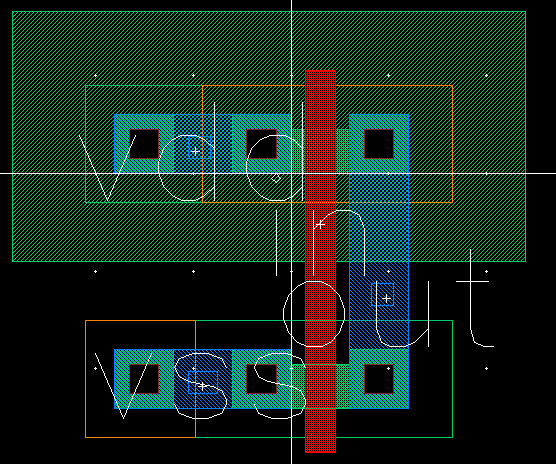
Now draw 2 more pins for vss and out, using M1 pin
Now, let’s place the pin in on the gate of the transistors
Left click LSW: Poly drw
Left click Editing: Create -> Pin…
Ensure all the switches are properly set and type in in the Terminal Names box.
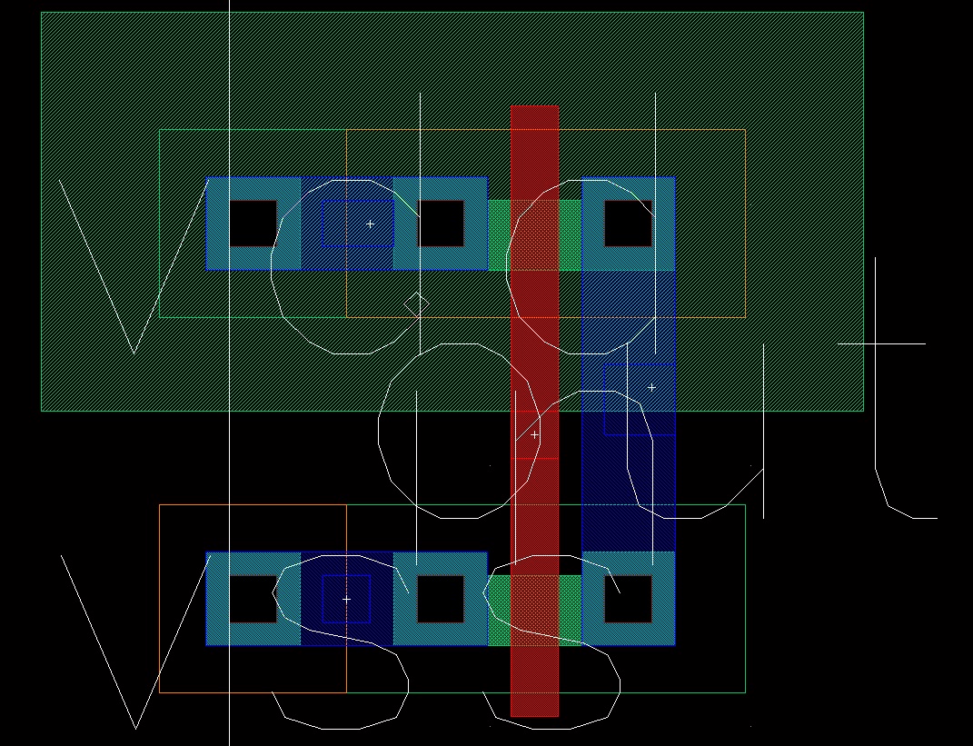
You have just finished the layout phase of the inverter. Save your design. Be sure to save early and often. It’s a guarantee that the first time you forget to save (especially in a big design after a lot of changes), the machine will crash and you will lose all your work. Your layout should look like the one below.