Bring up the schematic of inv_test. We need to replace the dc voltage input source with
a pulse source. Click on the vdc source that is connected to the input of the inverter.
The vdc should have a yellow box around it. Go to
Editing:Edit->Delete or press the Del button.
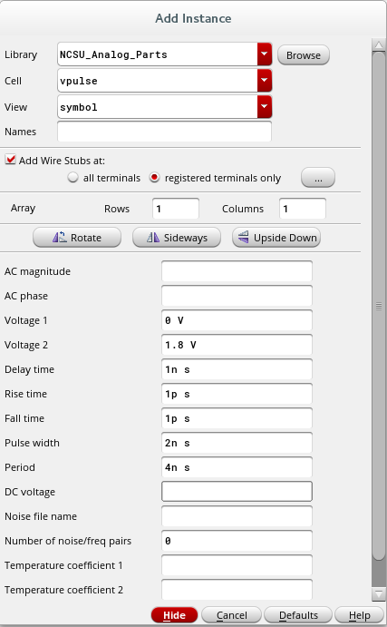
Left Click Add->Instance and select Cell Name: vpulse from Library Name: NCSU_Analog_parts and View Name:symbol. Fill the rest of the boxes as shown in the figure on the next page. The input pulse that we have specified is bounded between 0 and 1.8V. It has an initial delay of 1ns, rise and fall time of 1ps and high/low duration of 2ns.**

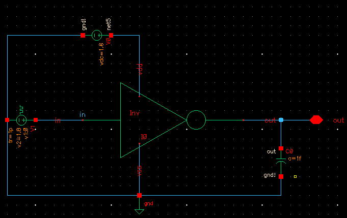
Place this symbol such that the positive end is connected to the input of the inverter. Refer to the next page for the end result.

Save the schematic. Left Click Editing:Design->Check and Save. After we have made these changes we are ready to run a transient analysis on the inverter.
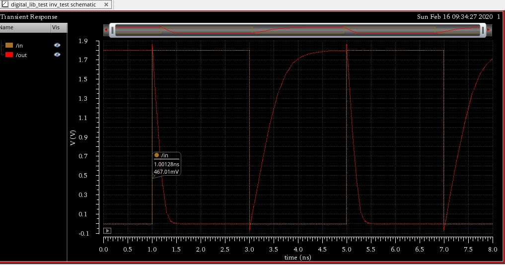
Left Click Editting:Tools->Analog Environment. In the ADE L window go to Analysis->Choose. Set the transient analysis with Stop Time as 8n. We have specified a transient analysis from 0 to 8ns.
Left Click Analog Environment: Outputs->To be Plotted->Select on Schematic. Select the input and output of the inverter. Refer to the previous section, DC analysis, for the necessary steps.
Run the simulation by pressing on the green traffic light icon and observe the results of the transient analysis. Now you can edit your results and print them out.
