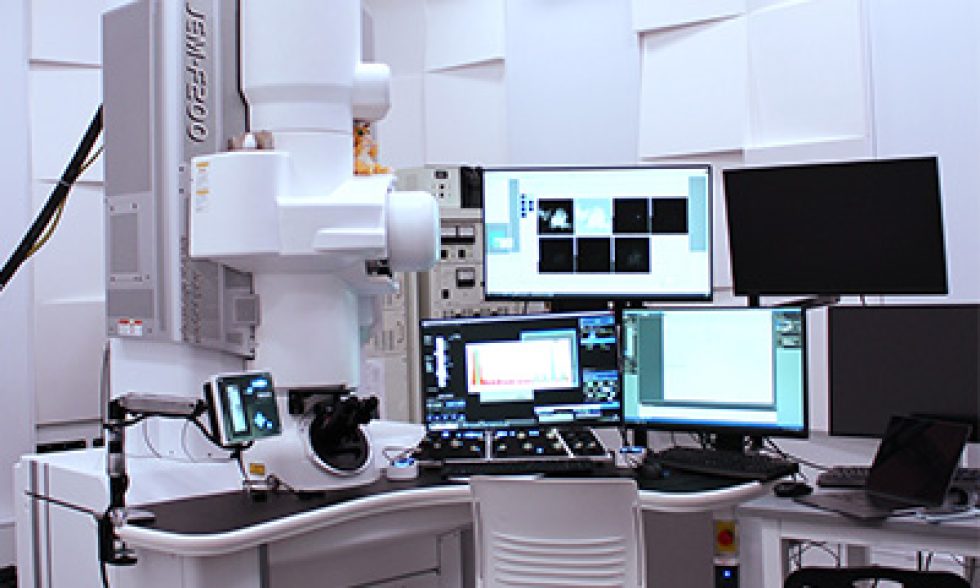
The MCP houses a JEOL F200 200 kV TEM that has 0.08 nm line and better than 0.2 nm point-to-point resolution. It is equipped with dual JEOL light-element detectors for quantitative X-ray analysis (EDX), scanning transmission electron microscope imaging with 0.14 nm resolution in both high-angle annular dark-field and bright field detectors. The F200 also has a Quantum Gatan Image Filter detector with a K2 electron detector for electron energy-loss spectroscopy (0.34 eV resolution). An IDES Luminary laser system is also available for illumination of samples with a laser. Added to all this is an ASTAR scanning precession electron diffraction system can generate maps of crystal orientations down to 2 nm. The F200 is also equipped with electron tomography holders and acquisition software. TEM holders available include double-tilt low-background holders for high-resolution TEM and EDX analysis, a heating and a liquid nitrogen cooled stage. A cryostage is available through the Integrated Imaging Center on campus.
- Dual EDX detectors for high throughput X-ray analysis and mapping
- Gatan K2-IS custom EELS system (Coupled with Gatan GIF Quantum Energy Filter);
- Gatan K3 direct detection camera for imaging
- NanoMEGAS Precession Electron Diffraction System with TopSpin;
- JEOL-IDES Luminary Micro: A Compact Specimen Photoexcitation System (CPXS) for JEOL TEMs. It is composed of a modulated laser, a compact optical delivery system (µODS), an inlet port, and a mirror. With this add-on, users can direct and focus the laser output onto the TEM sample in situ. With the Luminary Micro, users can study laser-induced phenomena in situ using fast cameras.
- Protochip Axon Dose and Data management
- JEOL IT700 FEG SEM – A compact and user-friendly SEM equipped with SE, BSE, EDAX EDX and EDAX EBSD detectors, and a spatial resoultion of 1 nm.
- The instrument is to get an internal laser system, for in-situ experiments with real-time characterization.

Location: Room G73A Stieff
Manufacturer: JEOL F200 200 kV TEM
Capabilities and Options: 0.7 nm line and better than 0.2 nm point-to-point resolution. 0.17 nm resolution in both high-angle annular dark-field and bright-filed detectors. Added to this is an ASTAR scanning precession electron diffraction and electron tomography.
*An SOP will be provided after training.
Contact

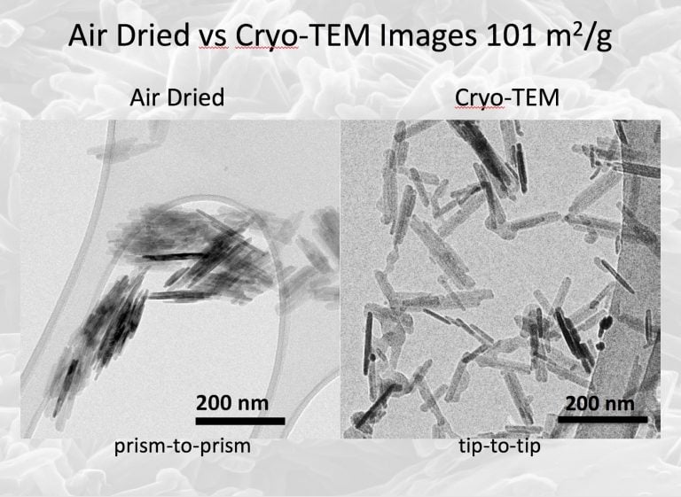
Cryo TEM of Goethite (alpha-FeOOH) (Livi, K.J.T., Villalobos, M., Leary,R., Varela, M., Barnard, J., Villacís-García, M., Zanella, R. Goodridge, A., and Midgley, P. (2017) Crystal Face Distributions and Surface Site Densities of Two Synthetic Goethites: Implications for Adsorption Capacities as a Function of Particle Size. Langmuir, 33, 8924-8932, 10.1021/acs.langmuir.7b01814.)

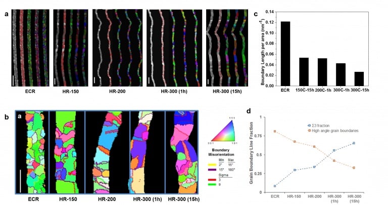
Scanning Precession Electron Diffraction (SPED) analysis of Cu metal nanowires (Raciti, D., Cao, L., Livi, K.J.T., Rottmann, P., Tang, X., Li , C., Hicks , Z., Bowen, K., Hemker, K., Mueller, T., and Wang, C. (2017) Low-Overpotential Electroreduction of Carbon Monoxide Using Copper Nanowires. ACS Catalysis, 7, 4467–4472, DOI: 10.1021/acscatal.7b01124.)


